


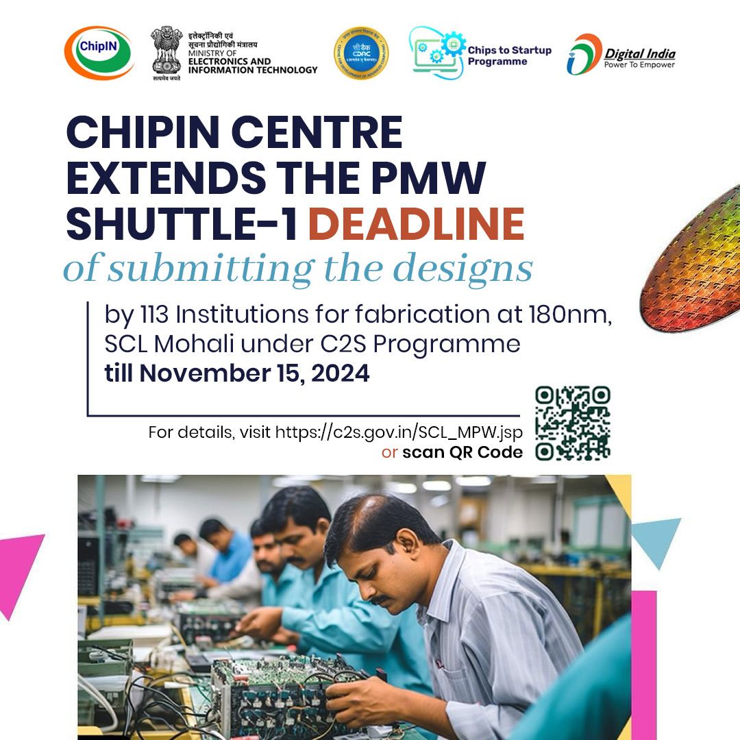
The ChipIN Centre at C-DAC Bangalore has extended the deadline for semiconductor design submissions for the first Multi-Project Wafer (MPW) Shuttle at 180nm technology, scheduled for fabrication at SCL Mohali.
Under the “Chips to Start-up” (C2S) Programme, 113 participating institutions (PIs) now have until November 15 to submit their designs, allowing more time to finalize details before the designs are sent for fabrication.
The Ministry of Electronics and Information Technology (MeitY) has established the ChipIN Centre at C-DAC Bangalore to support India’s semiconductor design community. This centralized facility serves as a one-stop hub, providing fabless chip designers from startups, MSMEs, and academic institutions with essential resources such as semiconductor design tools, fabrication access, and a virtual prototyping hardware lab.
Powered by cloud infrastructure, the ChipIN Centre offers advanced EDA (Electronic Design Automation) tools for the complete chip design cycle, and also coordinates fabrication services with Indian foundries, like SCL, as well as international foundries and packaging partners.
ChipIN Centre aims to accelerate India’s chip design ecosystem by supporting fabless chip design projects. It offers Multi-Project Wafer (MPW) services to academic institutions, startups, and MSMEs, enabling access to both domestic and overseas foundries. Designers have access to EDA tools from Synopsys, Cadence, and Siemens-EDA for integrated circuit (IC) design.
The facility also provides additional design services such as fab compliance checks, design validation, and integration, as well as coordinating packaging, chip characterization, and prototyping. Additionally, the ChipIN Centre will focus on developing a reusable IP core repository and offer EDA tool training. The facility also includes a Virtual Prototyping Lab at NIELIT Calicut for VLSI design training.
Timeline for MPW Shuttle-1 Process
- MPW Shuttle – I Announcement by ChipIN Centre for fabrication of designs at 180nm, SCL Mohali by Participating Institutions (PI) – 20 September 2024
- PIs to submit request to ChipIN Centre for obtaining the Silicon number from SCL. – 01 October 2024
- ChipIN Centre to provide Silicon number to the PI – 4 October 2024.
- Submission of the initial version of design by PIs to ChipIN Centre as per guidelines of Design Tapeout Submission Form (i.e. Si Number, report on DRC clean, antenna check etc.) – 15 November 2024.
- ChipIN Centre to provide a Verification Report to PIs for initial version of designs submitted by PIs – 19 November 2024.
- PIs to submit the final version of fab-ready design/ GDS to ChipIN Centre addressing the issues, if any, highlighted in the Verification Report – 29 November 2024.
- Submission of designs of PIs by ChipIN Centre to SCL for fabrication – 6 December 2024.
- The designs to go in the fabrication lot at SCL Mohali – January 2025.
- Receiving of fabricated designs in packaged form by the PIs – 31 September 2025.
Submission Requirements and Technical Guidelines
ChipIN Centre has set out specific guidelines for submitting design data:
- File Format: Only GDSII format files will be accepted, and send directly to ChipIN Centre by email.
- Design Layout and Naming: Layout grids must use a 0.005 µm grid size, and designs must follow a strict naming convention.
- Verification Checks: Before submission, institutions should ensure compliance with Design Rule Checks (DRC), density, and antenna rules. Verification includes MD5 and checksum validations for data integrity.
This extension in the C2S Programme aims to support participating institutions in refining their designs, aiding India’s broader goal of building a robust semiconductor ecosystem.
Also Read:


Discussion about this post