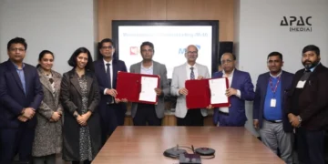
New Delhi: The Union Cabinet, led by Prime Minister Narendra Modi, on 14 May approved the establishment of a sixth semiconductor manufacturing unit under the India Semiconductor Mission.
This project is a joint venture between HCL Technologies and the global electronics giant from Taiwan, Foxconn. It marks a significant step forward in the country’s efforts to strengthen its domestic semiconductor ecosystem.
The newly approved semiconductor plant will be located near the Jewar Airport in the Yamuna Expressway Industrial Development Authority (YEIDA) region of Uttar Pradesh.
It will focus on producing display driver chips used across a wide range of devices, including smartphones, laptops, automobiles, PCs and other consumer electronics.
This HCL and Foxconn plant will be able to handle 20,000 wafers per month and will have the capacity to churn out 36 million chips monthly.
With five semiconductor fabs already under construction across the country, this latest approval reinforces the momentum behind India’s push to build a strategically vital chip industry.
The HCL and Foxconn semiconductor plant will see an investment of Rs 3,700 crore and is expected to significantly contribute to India’s goal of becoming self-reliant in semiconductor production.
Meanwhile, India’s semiconductor ecosystem is rapidly evolving, with world-class chip design hubs emerging across several states. Academic and entrepreneurial activity in the sector is surging, with over 270 institutions and 70 startups engaged in chip design and development.
Additionally, this should be noted that 20 student-led chip designs have already been taped out at the Semiconductor Laboratory (SCL) in Mohali.
Global supply chain partners are also expanding their presence in India. Leading equipment manufacturers such as Applied Materials and Lam Research have established operations in the country, while key chemical and gas suppliers, including Merck, Linde, Air Liquide and Inox are preparing to meet the growing demand.
Anurag Awasthi, a noted policy specialist and columnist in semiconductors and critical electronics, welcomed the development, calling it “an outstanding development” that the Union Cabinet has approved the sixth semiconductor facility, a joint venture between HCL and Foxconn. This announcement, he added, comes in tandem with the government’s recently unveiled Electronics Component Manufacturing Scheme.
“It is a first for Uttar Pradesh in line with a robust semiconductor policy launched in February last year. While the prowess of HCL is well known and Foxconn is a global IIDM (Innovation Integration Design Manufacturer), the venture will be a harbinger for many other joint collaborations between India and Taiwan.”
“In addition, the location will logistically cater to an easier movement of workforce, cargo, specialised machinery and much more as it is located in proximity to state-of-the-art Jewar airport, which is likely to begin full operations this year. While the facility is designed for a capacity of 20,000 wafers per month and can produce nearly 36 million display driver chips, there could be a large scope of capacity building as there could be more traction on volumes of production of mobile manufacturing in India with intrinsic benefits of single geography manufacturing, operations and distribution”


Discussion about this post