


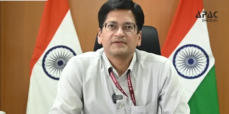
At the IndiaAI Impact Summit 2026, Amitesh Sinha, Additional Secretary, Ministry of Electronics and Information Technology (MeitY) and CEO of the India Semiconductor Mission (ISM), outlined India’s accelerating semiconductor roadmap, spanning fabrication, packaging, fabless innovation, advanced R&D, ecosystem development and market access reforms.
10 Semiconductor Units
Sinha said that India has cleared 10 semiconductor projects so far. “We have approved one silicon fab and eight packaging units. All of these 10 will start commercial production from this year, and they will attain full capacity by the end of 2028, 2029 and 2030,” he stated.
He added that approvals will continue under the next phase of the mission. “In the meantime, we’ll approve under ISM 2.0 many such projects, and some of them will again come because the period of setting a facility varies from two years to five years.”
Indicating expansion beyond the initial 10 units, he said, “So some of them will also come, so this 10 can become 15 or 17 or 18.”
Focus Shifts to Building Billion-Dollar Fabless Companies
While manufacturing and packaging remain priorities, Sinha emphasised that the current phase is strongly focused on nurturing fabless semiconductor firms.
“But this time our focus is to create a fabless company. So now the companies sitting here, the three candidates, C2i Semiconductors, Mindgrove Technologies and Marvell Technology, they are very, very promising and we want to see them as a billion-dollar fabless company,” he said.
Looking ahead, he projected the long-term ambition: “In the first phase, when ISM 2.0 will be over, 3.0 will start, but at that time, these companies, twenty-four companies, and the promising ones which are also coming now, you will see some of the fabless 1 billion company, and after that we want to see them as a Broadcom, Qualcomm, Nvidia, and all those kind of companies.”
He underlined the strategic intent behind the roadmap: “So, I’m setting this time and I’m very hopeful we are working very meticulously to see that all pieces of the puzzle are in place. So that anybody can build up their solutions, whether it is a design company or manufacturing company, a packaging company or equipment company or any kind of new technologies that can prosper in this country.”
From HPC to Advanced Nodes and Display Ecosystem
Sinha noted India’s changing capabilities in high-performance computing. He stated: “So whenever we talked about high-power computing earlier, it was not available to us. And now we are developing and now it is available to us also.”
On semiconductor nodes, he said India is currently moving across mature technologies. “Similarly, in future, we are doing 28 nanometers to 180 nanometers,” Sinha added.
He acknowledged that access to cutting-edge nodes remains challenging. “When we come down, probably technology will not be available. Though commercially it is available, all companies are setting up elsewhere, but perhaps they will not set up here. So should we wait for them or should we develop something?”
The government’s answer, he indicated, lies in proactive R&D investment: “So, now R&D, which the Government of India is focusing on, is all those kinds of technologies. Suppose you have an advanced node and you want to attempt 7 nanometer, 5 nanometer, 4 nanometer, 3 nanometer, then you want to have a display ecosystem. You want to attempt R&D in India because these technologies are quite guarded. So, unless LG and Samsung are coming to India, it will not come to India.”
He further pointed to emerging technology areas. Sinha said: “Similarly, we want to transfer data at a very high speed. So, whether you want to do it in silicon photonics or a similar kind of technology, there are various kinds of technology. So, in each of these technologies, which is very critical, whether it is quantum or any other kind of materials, we will now venture into that area.”
Strengthening the Semiconductor Ecosystem
Sinha stressed that ecosystem depth will determine India’s competitiveness. “Second is that the ecosystem is very, very important.”
He cited challenges such as global dependency for advanced processes: “So, tape out at TSMC will take a very long time. Getting a memory will take a very long time because there are many such ecosystem problems if they want to do a very critical 2-nanometer or below that, and they need a material of a specific nature…Again, material R&D is also important, so the ecosystem takes care of everything.”
On power management and thermal challenges, he said, “So now they are talking about power. So power dissipation is a very, very important thing. So, can you do something on diamond as a substrate or can you do something to dissipate heat? Because all these solutions will need such a kind of material and substrate.”
He revealed that several technology proposals are under review. “So we are seeing very good proposals in different technologies, whether it is GaN or on sapphire or silicon carbide in different flavors and then advanced packaging, again, a very, very important thing from today’s point of view. So we will approve many such projects, including R&D in material, equipment, and other things,” he noted
Highlighting the importance of manufacturing capability, Sinha added, “Precision engineering is also very important. So this will fill the ecosystem gap, narrow the timeline, and then the market access is a very, very important thing.”
Addressing commercialisation and procurement strategy, Sinha said there are two pathways to market access. “So there are two ways to gain market access: either the government is procuring or the government is not procuring. Where government is procuring, we can do many things,” Sinha said.
Leveraging national policy instruments, he added, “Because Make in India, there are a lot of provisions, and we are going to leverage that.”
For strategic applications, he indicated stronger domestic mandates. “So for all strategic applications, whether it’s defence or space, and you can define the strategic application depending upon our need, our security concerns, our different things. So in those areas, we can mandate something, and our startups, our innovators, our product developers can have access.”
On the commercial side, Sinha raised quality concerns. “On the commercial side, which is not directly covered under Make in India, there are many ways because we are getting a lot of substandard items and ultimately consumers are losing out on that. Suppose you are having a two-wheeler and your charger is not working; it is just because the standards are not good,” said the ISM CEO.
Sinha also said: “So we can impose many such conditions also to see that the credible stuff is coming to the country and there is a level playing field for our startups.”
EDA Support, Incentives and PLI
To strengthen startups, he detailed support mechanisms: “For providing that level playing field, we are now funding them. We want to be their partner. We want to give them all kinds of support in terms of EDA tools, which is the very first enabler for startups. EDA tools are very costly. And then we will also provide them with some incentive.”
He acknowledged the cost disadvantages faced by emerging firms, adding that “so once they are ready to run, at that point in time, because of sheer scale, where you are not matching to the fabless company of the world, probably the tape-out cost will be high. The marketing cost will be high. All those things are there.”
“To cover up those things also, we will provide certain PLI in terms of a level playing field for the startup,” he added.
Concluding on an optimistic note, Sinha said, “So all these things, I hope it will take care of much of their need and probably we’ll see a lot of fabless companies and unicorns coming from semiconductor.”
Also Read –
Invest India CEO Nivruti Rai Flags Massive Data Centre, Chip and Memory Gap at IndiaAI Impact Summit


Discussion about this post