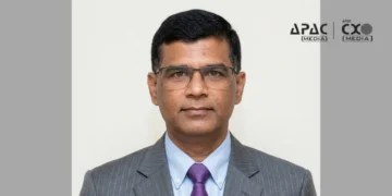





















IIT Kanpur has been on the path of advancing India’s technology frontier. Padma Shri Prof. Manindra Agrawal, Director, IIT Kanpur, in an exclusive conversation with Bhaswati Guha Majumder, Senior Correspondent at APAC Media, shares how the institute is working to position itself as the nation’s AI super hub while also driving grassroots solutions and defence innovations in drones and communications. He further emphasises the semiconductor push, startup collaboration to strengthen India’s ecosystem.
IIT Kanpur is known for its pioneering work for years. Could you share the key developments currently underway at the institute in areas like quantum technologies and AI?
In quantum technology, we have two large initiatives under the National Quantum Mission.
These are related to developing quantum sensing and quantum imaging. Quantum sensing is about developing a magnetometer that can detect extremely tiny magnetic fields at a level where every moving entity generates a very small magnetic signal. These quantum sensors can detect even that.
Using such sensors, one can pinpoint almost any moving object, with vast applications. For example, and this is still theoretical since nobody in the world has developed a working prototype yet, submarines could be detected underwater. Till date, submarines remain undetectable until they surface. With quantum sensors, that may change. Another application is navigation in environments where no external signals are available–quantum sensors can still help identify locations.
Similarly, quantum imaging offers exciting possibilities. For instance, one could take an X-ray of a patient sitting a thousand kilometres away. Two entangled photon beams are generated and taken far apart. One beam hits the patient, while the other beam is imaged. Whatever is in the patient gets imaged immediately, a thousand kilometres away. These are the kinds of applications possible once products emerge from these technologies. IIT Kanpur has already begun work in this direction.
On AI, we have recently established the Wadhwani School of Advanced AI & Intelligent Systems. Our aim is to become the country’s AI super hub, driving AI-based technologies across sectors such as healthcare, defence and governance. We have formed a strong group within this school to develop advanced AI-based solutions.
The IndiaAI Mission is currently focusing on building an indigenous LLM and has funded three startups, with more discussions underway. One of the startups has one of our faculty members as an advisor, so that’s one way we are involved. We are also part of the selection process for these startups.
IIT Kanpur’s portable soil testing device, Bhu-Parikshak, has been widely appreciated. Are there similar grassroots technologies in the pipeline?
Yes, we have several such solutions either under development or being commercialised. For example, Munh Parikshak, a non-invasive and radiation-free device to detect the onset of oral cancer.
Another technology can quickly detect water quality, while other techniques are designed to improve water quality.
Prototypes are ready and commercialisation processes are underway.
Defence technologies like the Analakṣhya Cloaking System highlight IIT Kanpur’s role in strengthening India’s self-reliance. Are there similar projects in the pipeline?
We are working on many defence technologies. A major focus is on drones–of various types, especially for military use.
We are setting up a major program to develop all critical drone components indigenously, including engines, motors, communication systems and cameras. These are essential for producing drones at scale and that’s the gap we aim to address.
We are also working on cybersecurity and communication technologies linked to drones. Quantum sensing, which I mentioned earlier, has serious defence applications as well. Quantum computing may take longer, but quantum sensing could be ready in the next five years, if all goes well.
With the government’s focus on developing a semiconductor ecosystem, how is IIT Kanpur preparing talent and research infrastructure to align with this national priority?
We are contributing in two main areas. First is packaging (generally referring to enclosing a chip in a protective package); we have a strong group working on chip packaging. Second is design, our faculty is working on novel designs and we are also supporting startups in this space.
While everyone talks about fabs, which are indeed important, setting up advanced fabs like 3-nanometer or 2-nanometer will take huge investments and time before setting up in India. Even the current facility underway is at 28 nanometers, with a roadmap to 10 nanometers. But beyond 10, the entire technology changes.
But design is something we are already good at and can do immediately. We can design circuits and devices for 3-nanometer or 2-nanometer technologies and get them ready for manufacturing in Taiwan. That’s where our focus lies, on the design side.