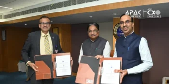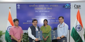


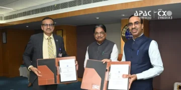
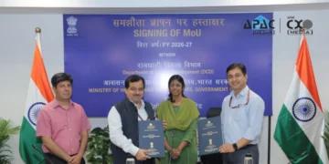



















New Delhi, May 29 (APAC Media): India’s semiconductor ambitions received a fresh boost after the Government of Odisha signed a Memorandum of Understanding (MoU) with Intel and 3DGS to introduce substrate manufacturing technology in the country.
Substrate manufacturing technology refers to the processes used to create the foundational base (the substrate) upon which electronic components are built, mounted, and interconnected.
Union Electronics and Information Technology Minister Ashwini Vaishnaw announced the development on Friday, describing the agreement as an important step towards strengthening India’s semiconductor ecosystem.
Congratulations to the Govt. of Odisha, Intel and 3DGS on signing an MoU to bring substrate manufacturing technology to India.
This will further advance semiconductor ecosystem in India. pic.twitter.com/elxs6r8muN
— Ashwini Vaishnaw (@AshwiniVaishnaw) May 29, 2026
The MoU is aimed at expanding India’s domestic chip manufacturing capabilities and strengthening the country’s electronics supply chain. Substrate manufacturing plays a critical role in semiconductor production, as substrates are used to connect and support semiconductor chips in electronic devices.
The announcement comes shortly after the Union Cabinet approved two major semiconductor projects under the India Semiconductor Mission (ISM). These include India’s first commercial Mini/Micro-LED display manufacturing facility based on Gallium Nitride (GaN) technology, along with a semiconductor packaging unit in Gujarat.
Combined, the two projects are expected to attract investments of nearly Rs 3,936 crore and generate employment opportunities for more than 2,200 skilled professionals.
The latest agreement also supports the Centre’s broader semiconductor roadmap unveiled earlier this year. In March, Vaishnaw had stated that four semiconductor plants are expected to become operational in India by 2026, while two additional plants are planned for 2027.
He had also indicated that India’s first semiconductor fabrication facility in Dholera is likely to begin operations by 2028.
“Our approach is design in India and make in India,” Vaishnaw had said earlier, while reiterating India’s target of becoming one of the world’s top six semiconductor nations by 2032 and among the top three by 2047.
Also Read:
SAIL, EdCIL Sign MoU to Promote Inclusive Education