


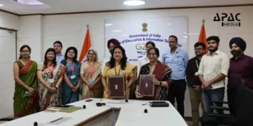


New Delhi: India has made substantial progress towards its target of training 85,000 engineers in semiconductor design over ten years under the government’s Chips to Startups (C2S) initiative, Union Minister for Railways, Information & Broadcasting and Electronics & IT Ashwini Vaishnaw said.
The C2S programme, launched under the India Semiconductor Mission (ISM), focuses on talent development through training, up-skilling and workforce development to strengthen the country’s semiconductor ecosystem.
According to the minister, world-class Electronic Design Automation (EDA) tools supported by companies such as Synopsys, Cadence, Siemens, Renesas, Ansys and AMD have been made available in 315 academic institutions across India. These tools enable students to gain practical experience in semiconductor chip design.
The chips designed by students are fabricated and tested at the Semiconductor Laboratory (SCL) in Mohali, providing hands-on exposure across the full semiconductor value chain, from design and fabrication to packaging and testing.
Vaishnaw said the initiative has evolved into the world’s largest open-access EDA programme, with more than 1.85 crore hours of EDA tool usage recorded so far for chip design training.
He noted that students from institutions across the country, from Assam to Gujarat and from Kashmir to Kanyakumari, are actively participating in semiconductor design activities, reflecting the growing nationwide engagement in advanced technology development.
Highlighting global industry trends, the minister said the semiconductor sector is expected to grow from its current size of about $800–900 billion to nearly $2 trillion, which could create demand for around two million skilled professionals worldwide.
To further strengthen talent development, Vaishnaw announced that under India Semiconductor Mission 2.0, the programme will be expanded from 315 to 500 academic institutions. The move aims to create a steady pipeline of skilled professionals in semiconductor design, fabrication, packaging and testing across all states.
He reiterated that the government remains committed to building a self-reliant semiconductor ecosystem through talent development, infrastructure expansion and industry collaboration, positioning India as a global semiconductor hub.


Discussion about this post